If you do not pay careful attention to the excellent construction of your printed circuit board (PCB), then it will cause a great deal of difficulty in the process of developing the PCB. As a consequence of this, your board is now capable of being manufactured, which results in a poor ratio and also has the potential to cause early failures out in the field. You need to have a solid understanding of the PCB manufacturing process to produce a PCB of high quality, therefore let’s look into the post and learn more about it. It is a complete waste of time to go right into the work of manufacturing without having a thorough understanding of the many procedures involved and the connection between the schematics and the idea. Let’s go through a few of the words that are utilized while discussing the PCB prototype.
PCB development
It is believed that the process of developing a printed circuit board (PCB) is the procedure of taking a PCB board design from its manufacturing design. Three steps make up the PCB design process, and they are referred to as design, fabrication, and testing respectively. The primary objective of this procedure is to produce a printed circuit board (PCB) design of the greatest possible quality within the allocated amount of time for its development, and you must produce a developed PCB within this time alone.
PCB manufacturing
The production of printed circuit boards (PCBs) is also included in the building of board designs. The production of printed circuit boards (PCBs) is a two-stage process that begins with the fabrication of the board and concludes with the assembling of the circuit boards.
Examination of PCBs
The testing of PCBs is sometimes considered to be the third step of the creation of PCBs. In most cases, this stage comes after the production process has been completed. PCB testing has been completed to evaluate the capability of the board to carry out the operational functionality that it requires. In this step, if any flaws are discovered in any part of the design, then it has to be fixed and enhanced properly so that it can fulfill the requirements and demands of the program.
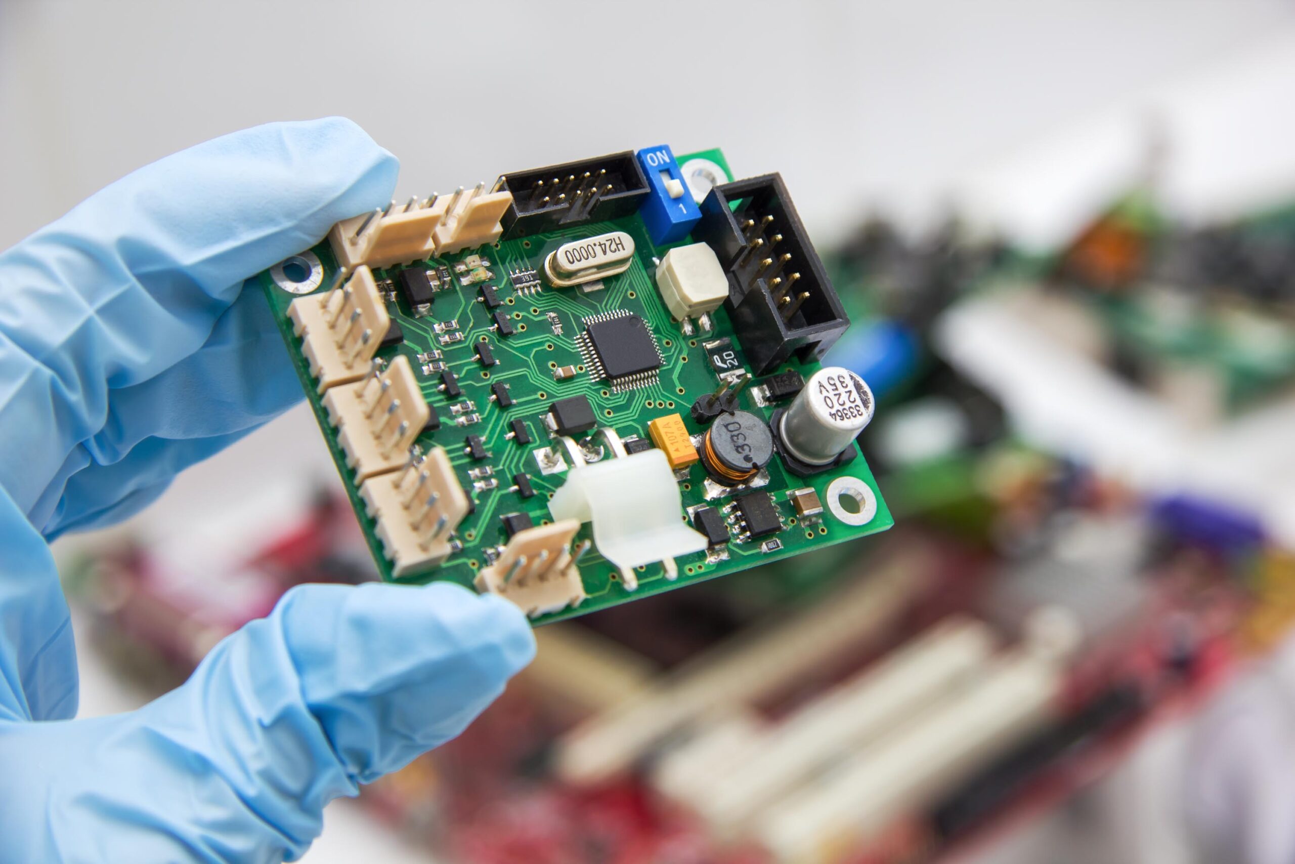
Assemblage of PCBs
In the second step of PCB manufacture, components are soldered to the board.
PCB factory manufacturing uses the design package’s specifications to create a real circuit board. The following primary steps will result in the achievement of the desired physical structure.
- Creating an image of the arrangement using copper laminates.
- Inner layers are stripped of copper to disclose pads and traces.
- The formation of the PCB layer involves laminating the boat material and then pressing it while it is heated to an extremely high temperature.
- The plating of the pinholes is the next phase in the process.
- You will need to apply an additional layer of protection to the surface.
- Logos, markings Screen printing is done using silk on the surface.
ChinaPCBOne Technology LTD. is the author of this article on PCB prototype. Find more information, about PCB manufacturer.