The usage of HLC (High-layer Count) PCB boards, which incorporate critical characteristics such as skip vias, POVF fabrication, sophisticated raw materials, and impedance management, is one viable solution to the requirements of 5G technology.
Special attention must be devoted to PCB manufacturing, design, and production to fulfill the demands of 5G era applications and beyond. PCB size and thickness, dependable vias, precise registration, reliable and accurate manufacturing procedures, signal integrity, and effective raw materials are all issues that must be addressed starting in the design phase and continuing through manufacture.
HLC PCB boards with critical features including skip vias, POVF fabrication, improved raw materials, and impedance management are one effective way to meet the demands of 5G technology.
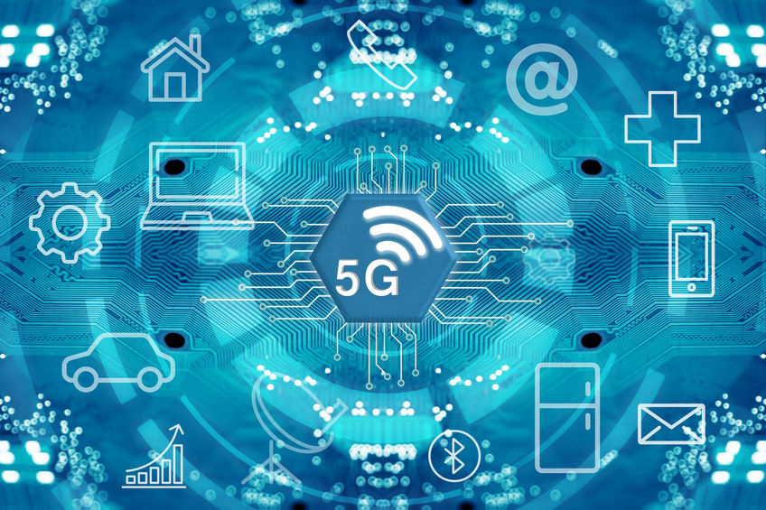
PCB Changes in the 5G Era 5G requires significantly more advanced component integration, such as antennas. As a result, there’s a demand for smaller components to help integrate. Furthermore, high-frequency materials and tight RF trace tolerance are now required for antennas.
Furthermore, because the transmission power of 5G base stations is much larger than that of 4G, solutions that can achieve lower losses and better thermal management while still enabling high-speed, high-frequency solutions with dependable signal integrity are required.
Another approach to look at the 5G issues is to focus on three essential performance aspects that PCBs must provide:
* High speeds * Fast transfer rates * Low losses
Engineers have discovered that HLC PCBs are an ideal way to handle the stringent criteria of 5G technology. HLC PCBs already support size limits and manufacturing procedures such as accurate registration and dependable vias. Engineers have established, however, that they can improve signal integrity and impedance management and implement raw high frequency and low-loss materials.
PCBs with HLC
HLC PCBs, which refer to circuit boards having 12 or more layers, is one way to keep ahead of the 5G adoption curve. These PCBs prototypes are thicker than standard PCBs, and they frequently have a huge panel size with a small hole drilled in the rear.
Impedance management and insertion loss are crucial for these PCBs to deliver the required performance.
HLC PCBs: Considerations
As previously said, there are a few aspects to consider while using HLC PCBs to achieve the correct levels of performance required for 5G applications:
- Impedance Control
- Upgraded Raw Materials
- Skip Vias
- Layer to Layer Registration
- POVF
- Impedance Control
- Vias should be avoided.
Making interconnections via numerous layers is one of the hurdles in manufacturing functional HLC PCBs. Because they can flow through numerous layers without establishing electrical contact with each one, skip vias have become necessary. These vias are vertically laser drilled, as are most vias, and require high precision, although the technique is highly complicated if satisfactory results are attained.
Registration from one layer to the next
The significance of tight layer registration tolerances in HLC PCBs cannot be emphasized. Temperature, humidity, and the quality of registration hole placement can cause registration and alignment to be distorted throughout manufacture. Extremely tight registration tolerances can be achieved thanks to careful selection of production methods and calibration of crucial equipment.
POVF
In pad, a procedure known as POVF (also known as VIPPO or VIA) is frequently used to reduce board space by decreasing hole spacing and holes while also boosting wiring density. This helps reduce the board’s footprint and achieve a lighter-weight solution without sacrificing performance. And, more crucially, it performs admirably when using skip vias. POVF is more difficult to manufacture, but it produces a considerably more dependable and accurate HLC PCB.
Controlling Impedance
When high-frequency signals propagate across PCB signal traces, as they frequently do in 5G applications, the traces effectively become transmission lines. Each point on the signal trace has its own impedance, and signal distortion can occur when there is a difference in impedance from one point to the next. PCB manufacturing must be built with impedance management to maintain signal integrity.
Materials that have been upgraded
Upgraded raw materials are also required due to the high data rates involved. High-speed materials like TU862, a halogen-free epoxy resin composite, and E-glass fabric are among them. This is a medium-loss material that is frequently used in 14-layer PCBs.
Another example is S7439, a low-loss material that may be utilized with ten layer PCBs. M6G is a very low loss material, whereas M8 is an ultra-low loss material. There are hydrocarbon-based solutions like Aerowave 300 and PTFE-based options like Rogers TC350 for applications that demand high-frequency materials.
PCBs with HLC: 5G and Beyond
A large number of layers As 5G technology advances, PCBA manufacturing prototype will become increasingly important. The primary solutions for delivering the performance and reliability necessary for 5G include speed and losses related to the chosen raw materials, high accuracy and low tolerance manufacturing procedures, and signal integrity.
Other applications that potentially benefit from these methods include:
* File servers * Data storage * GPS technology * Satellite systems * Weather analysis * Medical devices
ChinaPCBOne Technology LTD. is the author of this article on PCB Prototype. Find more information, about PCB Manufacturing.